In this section you will able to learn how to write the Verilog code for basic code in data flow model and its Testbench for functional verification of all gates.
Structure
The figure below show the all basic gates structure of NOT GATE, OR GATE,AND GATE,NOR GATE ,NAND GATE,XOR GATE,XNOR GATE.

NOT GATE
not gate inverts the input. not gate has one input.
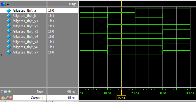
input a=0 ,output y1=1 and when input a=1,output y1=0.
OR GATE
when any one input of OR Gate is 1 then output will be 1.for two input or gate truth table will be as given below
a=0,b=0 then y2=0
a=0,b=1 then y2=1
a=1,b=0 then y2=1
a=1,b=1 then y2=1
AND GATE
when any one input of AND is 0 then output will be 0.for two input AND gate truth table will be as given below
a=0,b=0 then y3=0
a=0,b=1 then y3=0
a=1,b=0 then y3=0
a=1,b=1 then y3=1
NOR GATE
for two input NOR gate truth table will be as given below
a=0,b=0 then y4=1
a=0,b=1 then y4=0
a=1,b=0 then y4=0
a=1,b=1 then y4=0
NAND GATE
for two input NAND gate truth table will be as given below
a=0,b=0 then y5=1
a=0,b=1 then y5=1
a=1,b=0 then y5=1
a=1,b=1 then y5=0
XOR GATE
when both input of XOR GATE is same then output will be 0.for two input xor gate truth table will be as given below
a=0,b=0 then y6=0
a=0,b=1 then y6=1
a=1,b=0 then y6=1
a=1,b=1 then y6=0
XNOR GATE
XNOR is invert of XOR GATE hence it will give output inverse of XOR Gate. for two input XNOR gate truth table will be as given below
a=0,b=0 then y2=1
a=0,b=1 then y2=0
a=1,b=0 then y2=0
a=1,b=1 then y2=1
Verilog code using data flow model

Testbench for the above module

Simulation Results
Top Level view of Design

in this case Testbench is connected to module (dut).Testbench will give input to the design and we will see the output of dut on wave. when you double click on dut you can see the design schematic view of all gates.


Comments
Post a Comment